

PCB to circuit diagram
Sometimes you need to convert from PCB to circuit diagram.
I have often thought about this problem but never undertook the task. This time I had just the project to give it a go. I’ll show you how I went about it.
It happened almost by accident. I had been trying to figure out how the Sequential Circuits Pro 1 envelopes sounded so good compared to some other envelope generators. They were using the same CEM3310 IC so I was building up the Pro 1 circuits that I came across on the internet. Unfortunately following the Pro 1 circuit I was unable to come up with anything usable. The times were way too short. Nothing like a Pro 1 anyway.
I found a project for Pro 1 envelope generator and looking at the parts list they were doing it pretty much like I had with a -5 volt supply. There were no circuits so I bought the project to reverse engineer and build.
This way I would hopefully firstly work out what I was doing wrong and secondly end up with a euro rack Pro 1 envelope generator. A win win all round.
That was as long as I could figure out what the circuit was from the PCB!
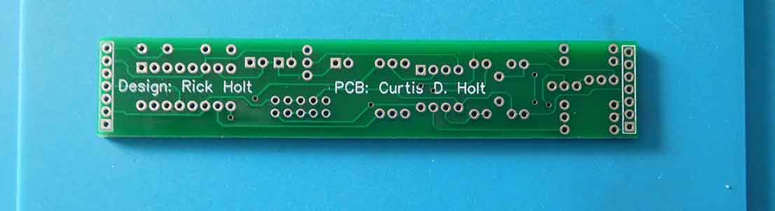
This is the PCB that I wanted to get the circuit diagram from. This is the track side.
The PCB was double sided and not too complex so I thought id give it a go. The first step was to look at the component list, in fact not just look at it but print it off. This was followed by a print off of the data sheets and pin outs of the integrated circuits, transistors and regulators.
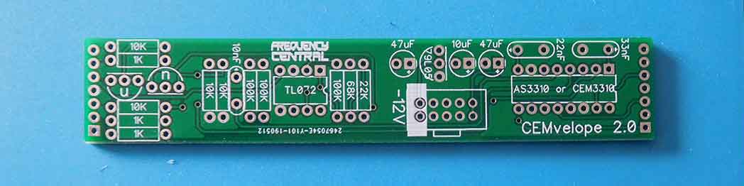
Using the data sheets you can find out where the power connections are. This should be fairly straight forward. You’re also going to need some sheets or paper for your working outs.
PCB to Circuit diagram steps
I’ll go through the steps I did with my specific example.
I made a sketch of the PCB with the components places. You could do a scan of print off a photo to save time. I then used two different coloured highlighter pens to draw in where the tracks went so how the components were connected. Two different colours were used where connections crossed so I didn’t look back on it and think they were connected.
You’ll need a continuity tester of some kind. You’ll probably have one on your multi meter. You will also find it easier if you have one that beeps to give you an audio signal so you won’t keep having to take your eyes off the board to read your meter.
If there are voltage regulators on the PCB once you have identified them you will know which connection is 0V and which is the voltage output. You can then use the tester to identify all the 0V connections and mark them on the component diagram. You can also do the same for the positive and negative rails if there are any. My board had a 79L05 so I was able to find the 0V and -5V connections.
You can then go round all the pins of the IC’s and mark all the various voltage and 0V pins.
Using the data sheet for the CEM3310 you can see where other components are connected. For instance two timing capacitors are used on pins 1 and 8 and there are capacitors on the board in that area. A community check confirms they are the ones connected to the correct pins and then 0V.
Visually look where the tracks go
It’s then a question of following the tracks visually on the PCB. Then using the continuity tester to verify what you are expecting and what is connected. This is a sort of balancing act.
Using a continuity tester and looking at the tracks I was soon able to mark all the physical connections.
This method is a lot easier than trying to use the continuity tester and draw a circuit diagram from the results. I know this because I tried it and didn’t get very far without making mistakes. It’s easy to lose track of which component you were looking at when drawing the circuit.
Once you have the diagram you’ve just made its a lot easier to go from this to a circuit diagram as all the connections are there to start with and you’re not messing with the continuity tester as you go along with trying to draw.
Start to draw up your circuit
Once I had this component diagram with all the connections marked I started to draw up a circuit diagram.
I knew the inputs were the gate and trigger. Following from the sockets you could see the both went thought resistors and to transistors. Using the pin out diagrams for the transistors it was easy to draw out what was a pretty standard transistor circuit with power going to the collector and the emitter going to 0V via 10K resistors. These connected to where The CEM3310 data sheet indicated. The other IC was the dual op amp and again using the data sheet and drawing them up by following the connections from my component diagram the resistors surrounding it and the connections to 0V made a pretty standard configuration of the two op amps acting as inverting buffers so one buffered the voltage out of the CEM3310 and the other inverted it.
Summing up going from a PCB to circuit diagram.
When you first start I can all get a bit overwhelming. It’s almost like doing a puzzle. Once you start drawing components in place it makes it easier to see where the others go. First step is to draw in the connections from the PCB image. Then using this diagram go to drawing out a circuit. Using data sheets you can see where you are expecting components to connect. There are various building blocks that you can identify and you will know how NPN and PNP transistors are connected, along with op amps.
The next stage for me is to build up this circuit on breadboard to fully test it out. I have another article How to build a circuit on a breadboard if that is something you are looking to do. It contains details and some helpful tips and advice to help you get a working circuit.